CÔNG TY TNHH THIẾT BỊ KHOA HỌC KỸ THUẬT AN DƯƠNG
info@adgroup.vn

Giá bán: Đang cập nhật
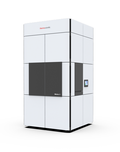
Liên hệ ngayNanoprobing for
electrical fault isolation and efficient TEM workflows to improve semiconductor
failure analysis.
Applications
Semiconductor Advanced
Packaging
Semiconductor research
and development
Semiconductor Failure
Analysis
Semiconductor power
devices
Semiconductor
materials characterization
Key Features
Leading edge transistor probing
nProber IV SteadFast
Nanomanipulators and temperature-controlled probing environment combine to give
the probe the necessary stability for working with leading-edge transistors.
High-resolution imaging of sensitive samples
The new LEEN2 Column
of the nProber IV System enables low eV imaging and probing operation and
includes an advanced control system that reduces sample dose by up to 30%.
These advances allow the nProber IV System to provide accurate measurements of
critical transistor parameters with minimal shifts from SEM imaging.
Guided operation and automation
The nProber IV System
is equipped with eFast semi-automated guided workflows that take you through
system operation from sample loading to electrical characterization. eFast
Software automates the setup of the LEEN2 Column and controls key sub-systems
ensuring consistent results in a multi-user production environment.
3D structures
The nProber IV Systems
can be equipped with EBIRCH2 and EBAC to find critical faults in 3D
interconnect structures down to ~100 Ω. EBIRCH2 can also be used to localize
critical defects in FinFET transistors.
In addition, the
nProber IV System can be equipped with a sub-stage that enables probes to be
separated by many millimeters, essential for the isolation of faults in large
3D NAND structures.
Resistive gate faults
The nProber IV Systems
can isolate resistive gate faults utilizing high-speed pulsed probing with rise
times of less than 1 ns.
Automation
Our easyProbe Software
automates key steps in the nProber IV workflow including: cleaning the probes,
lowering the probes to the sample, and optimizing the electrical contact
between the probes and the sample. easyProbe Software significantly reduces the
training required to use the nProber IV System and allows for extended periods
of unattended operation.
Automotive reliability
The optional Thermal
Characterization Package supports the most recent automotive reliability
standards. Samples temperatures can be controlled from -40°C to 150°C in order
to isolate faults that are not detectable at ambient temperatures.
Techniques
Nanoprobing
As device complexity
increases, so does the number of places defects have to hide. Nanoprobing
provides the precise localization of electrical faults, which is critical for
an effective transmission electron microscopy failure analysis workflow.
Sample Preparation of Semiconductor Devices
Thermo Scientific
DualBeam systems provide accurate TEM sample preparation for atomic-scale
analysis of semiconductor devices. Automation and advanced machine learning
technologies produce high-quality samples, at the correct location, and a low
cost per sample.
Device Delayering
Shrinking feature
size, along with advanced design and architecture, results in increasingly
challenging failure analysis for semiconductors. Damage-free delayering of
devices is a critical technique for the detection of buried electrical faults
and failures.
For more detail information of nProber IV System, please visit the website:https://www.thermofisher.com/vn/en/home/electron-microscopy/products/electrical-failure-analysis-systems/nprober-iv.html#features
Or directly contact to ADGroup