CÔNG TY TNHH THIẾT BỊ KHOA HỌC KỸ THUẬT AN DƯƠNG
info@adgroup.vn

Giá bán: Đang cập nhật
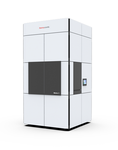
Liên hệ ngay Lock-In IR Thermography system for localization of defects in semiconductor devicesApplications
Semiconductor Advanced
Packaging
Semiconductor research
and development
Semiconductor
metrology
Semiconductor Failure
Analysis
ESD Semiconductor
Qualification
Semiconductor power
devices
Semiconductor display
technology
Semiconductor
materials characterization
Key Features
Very high sensitivity,
InSb camera, and thermal emission optics enable nondestructive,
through-package, and stacked die analysis
Real-time lock-in
measurement
Contactless absolute
temperature mapping
Optical beam-induced
resistance change (OBIRCH) option
High-voltage power
device analysis option (VX)
Specifications
|
Lateral resolution |
Down to 1 μm |
|
Depth resolution |
Down to 20 μm |
|
Defect types |
Wide range of shorts (2 mΩ to 2 GΩ), leakage (power
dissipation as low as 1 μW), resistive opens |
|
Sample types |
Board assemblies, modules, packages, full wafers, wafer
coupons, die |
|
FOV |
Max 200 mm x 160 mm; min 0.62 mm x 0.51 mm |
|
DUT stimulation |
Internal DC power supply; ATE, CA bus, boundary scan tester,
system level tester Up to 10 kV capable (requires VX option) |
|
Time to results |
Minutes to seconds, depending on applied power and sample |
For more detail information of ELITE System, please visit the website: https://www.thermofisher.com/vn/en/home/electron-microscopy/products/electrical-failure-analysis-systems/elite.html#features
Or directly contact to
ADGroup